I have a couple projects that I want to do that use ATMEGA328 chips. One is available as a kit here, but I’d like to learn the process of making a board. Does anyone have any experience with this? I have the .brd and .sch files, but haven’t the first clue what to do with them.
The short answer is yes, several of us have experience with this.
Are you looking to etch it yourself, or send it off to be printed?
There are lots of tutorials to get you started at http://www.instructables.com/tag/type-id/?sort=none&q=printed+circuit+board for both options. If the .brd layout you have is double sided, then etching it would be much more difficult, and you might want to start with having it printed for you.
For getting it printed, I recommend oshpark.com, where the “learn to solder” badges come from. What you would need to do is generate a “gerber” file, a zip file that contains images for each of the layers. He charges $5 per square inch (including shipping) and you get three copies of the board, the same purple soldermask and gold tracings as on the badges.
http://hackaday.com/2009/01/15/how-to-prepare-your-eagle-designs-for-manufacture/ outlines the process pretty well.
I’m making the assumption that the .brd and .sch files you have are for eagleCAD, but you certainly don’t have to use that package. Did you design it yourself or download those two files from somewhere?
I’ll add that the hackaday tutorial was made in 2009. The information one where to get it printed and how much it costs is out of date. For everywhere that it talks about batchPCB, substitute Oshpark.com, who took over all their business. When it talks about using the sparkfun design rules, you can substitute the ones oshpark.com provides. http://oshpark.com/guidelines
Here is an even simpler tutorial on making gerber files for oshpark from eagle. http://support.oshpark.com/support/articles/134816-generating-custom-gerbers-from-eagle
The faq also notes you can just upload eagle .brd files directly and they will figure out what to do. I’ve never tried this, I tend to want to tightly control what layers make it onto the silkscreen and what don’t, but that certainly would be the simplest option. But then you wouldn’t have really learned much about the process at all.
I have uploaded a couple of boards to oshpark directly from eagle and have been very satisfied with the results. However, if you go with 4 layer in eagle (which my latest project does, for density reasons) you have to go to gerber first. The best thing you can do when you have to go through that step is get a gerber file viewer and load up your output and make sure stuff aligns. It pays to understand what’s going on behind the scenes but it’s not required to do so.
I downloaded the files from an instructables project. I believe it is a 2 layer board, but I’m not sure. I assume that layers refer to traces and not silk screen. Is that correct?
Since it is 2 layers, I think I’ll take the easy route and have it printed, but I really don’t need 3. So I might just buy the kit for this one unless having the boards printed is more cost effective.
The other project is a guitar tuner, and the instructions are written for perfboard, so maybe I’ll try and design a board for that.
You are correct. The layers refer just to the copper. When you make a gerber file, you actually create 6 or more files that include things like silkscrens and soldermasks, but only the copper ones are the ones referred to usually for pricing.
Jon -
Just for chuckles, Jon Neal and I attempted etching a board using the laser cutter this evening. We need to tweak the process a bit, but initial results are very promising. It looks like a viable approach for single sided boards, and we have all the required materials at the hive.
This might be interesting to play with on the next Microcontroller Monday. Bring your board files if you come.
I have done the laser cutter/paint technique a few times. It's my goto for quick single layer protos. If you have any questions I will be happy to answer them, but there isn't much to it except making sure you use many layers of paint. I use a minimum of five light coats.
j
I sent the metronome board off to OSHPark, but I'd like to do the tuner board. My main problem right now is creating the board files. I have a JPEG of the schematic, but I'm having issues recreating it in eagle and/or fritzing. Also the project is using an arduino uno. I think I could integrate a bare bones arduino into he board, but I have no idea how to do that. Remember, I'm new to electronics. I can read schematics a little but have trouble converting them to a physical circuit and vice versa. I think I'll head to the hive around noon to work on the schematic(less distracting than home). maybe I can snag some pointers if someone is there, otherwise I'll plan on coming to micro controller Monday.
Anyway, the laser etched board sounds intriguing.
It probably won’t help that much until you get a little more comfortable with eagle cad, but here is the base minimal arduino schematic that I use as a template when making arduino compatible things. I got tired of figuring out every time so I made this as a starting point.
bare arduino.sch (331 KB)
Thankee sai.
At the risk of sounding stupid, where is the light switch for the main/table area?
All the way in the back to the left of the double doors. Take care not to trip over the layers of steel tube in the center of the room.
And there was light!
OK, I’ve completed most of the schematic, but I am not able to connect the power to my op amp in the schematic. Pins 4 and 8 are not there (see pics) sch.png is from my schematic in eagle, and tuner.png is from the original schematic on instructables.com. I’m confuzzled.
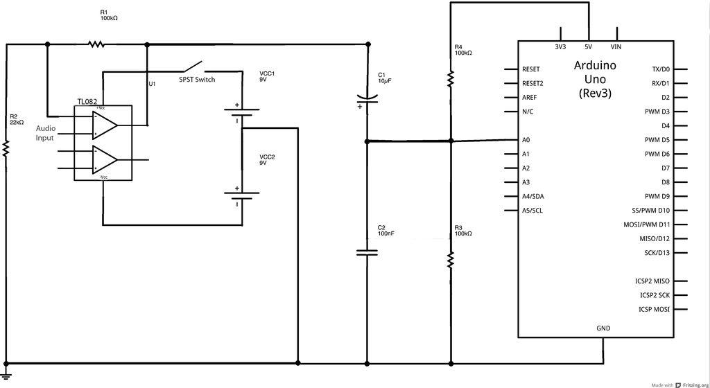
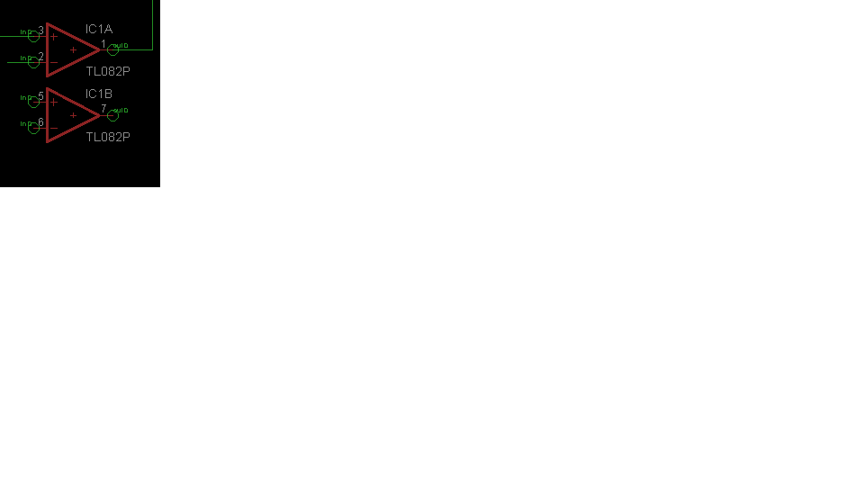
Are you sure you have exactly that model op amp? I believe that chip has TWO op amps built in but your schematic only needs one of them, so the extra one (on pins 5,6 and 7) is just not used. If you have a different chip the pins may be different.
Or do you mean the schematic isn’t showing how to use pins 4 and 8? When in doubt, find the datasheet (and then cultivate the ability to ignore most of it as confusing). http://www.datasheet4u.net/download.php?id=321275 tells me that pin 4 would be -VCC and pin 8 is +VCC.
I just can't see how to attach the net to pins 4 and 8 within eagle. Pins 4 and 8 are not displayed in schematic view, but they are present in the library info. as - and + VCC
Those two pins are already connected to Vcc/Gnd for you automatically (not sure about Vcc; could be another power net)
I just can’t see how to attach the net to pins 4 and 8 within eagle. Pins 4 and 8 are not displayed in schematic view, but they are present in the library info. as - and + VCC
OK, have a look at my files, you’ll see there is no pin 4 or pin 8 to connect to. As a result, there will be no traces connecting from power to pins 4 and 8 on my board. Also pay no attention to the layout, It’s nowhere near the final placement.
If you want to have a look at the project, I’m trying to reproduce this:
http://www.instructables.com/id/Arduino-Guitar-Tuner/?ALLSTEPS
Tuner.brd (90.2 KB)
Tuner.sch (903 KB)